General Description
FSMOS® MOSFET is based on Oriental Semiconductor’s unique device design to achieve low RDS(ON) , low gate charge, fast switching and excellent avalanche characteristics . The high Vth series is specially designed to use in motor control systems with driving voltage of more than 10V .

Features
|
|

Applications
|
|
Key Performance Parameters
|
Parameter |
Value |
Unit |
|
VDS |
150 |
V |
|
ID, pulse |
720 |
A |
|
RDS(ON), max @ VGS =10V |
7 |
mΩ |
|
Qg |
107 |
nC |
Marking Information
|
Product Name |
Package |
Marking |
|
SFS15R07PNF |
TO-220-3L |
SFS15R07PN |
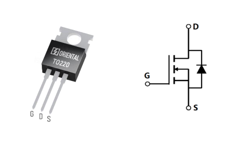
Package & Pin Information
Performance Parameters
Package
TO-220-3L
Cfg.
N
VDS (V)
150
VGS (V)
20
ID (A) && Tc=25℃
180
Ron (Ω) && 10V
0.007
-
文件大小: 920.5KB

工业连接器
工业连接器